Enabling Realization of Oxide Electronics
Business opportunity
Leading scientists at the Dept. of Chemistry, Univ. of Oslo have developed a production method for materials with very high conductivity targeting the key challenges in the electronics industry: Enabling significant reduction in component size, energy consumption and heat production in both consumer electronics and specialized electronic products. The technology can represent a door opener for the realization of oxide-based electronics as it can
- Enable realization of SrTiO3 as the highly awaited high-κ material for next-generation transistors
- Impact design of memristive electronics enabling neuromorphic computing
- Enable more robust electronics with respect to temperature and chemical environment (e.g. military, space, oil&gas)
- Be utilized as electrode material in oxidative environments and used in catalysts, fuel cells, and electrolyzers
Inven2 seeks partners for co-development and/or licensing of the technology. We are interested to validate the technology applicability together with user partner.
Technology description
Direct epitaxy of LaNiO3 films on SrTiO3 (STO) is demonstrated at 225 °C (Figure), where the films show surprisingly good properties: Metallic at all temperatures, conducting with low resistivities (<100 µΩ cm) with high carrier concentration (>1022 cm-3). The method used is Atomic Layer Deposition (ALD) with a novel process design. The films can be conformally deposited on large wafers (>8 inch, reactor limited) with high aspect-ratio morphology. This enables high-volume production and low prices.
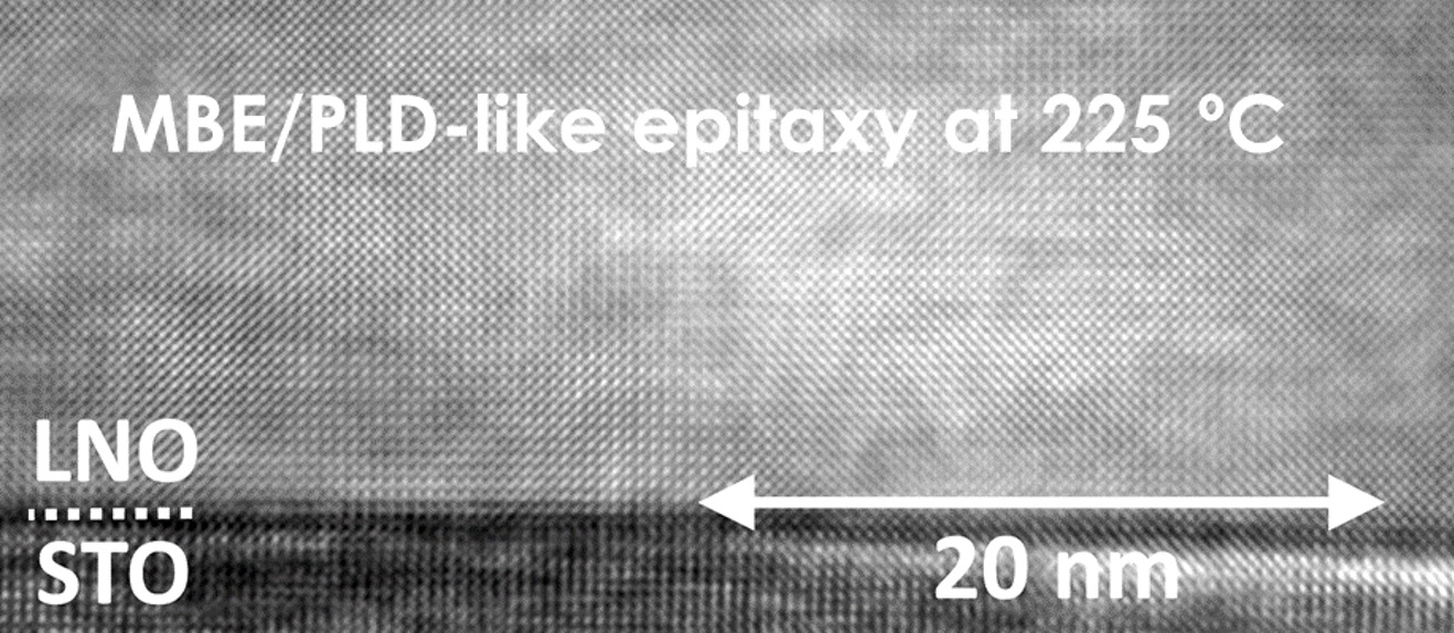
STEM image of a 30 nm LaNiO3 thin film on SrTiO3 substrate, exhibiting near defect free epitaxy.
Advantages
The new method enables formation of high-quality materials of compounds such as LaNiO3 (LNO) and SmNiO3 at very low thermal budgets (225 °C) as compared to the >700 °C required by alternative approaches. This significant drop in thermal budget opens for implementation and integration into process lines for silicon-based electronics.
IPR
PCT/GB2020/051724.